

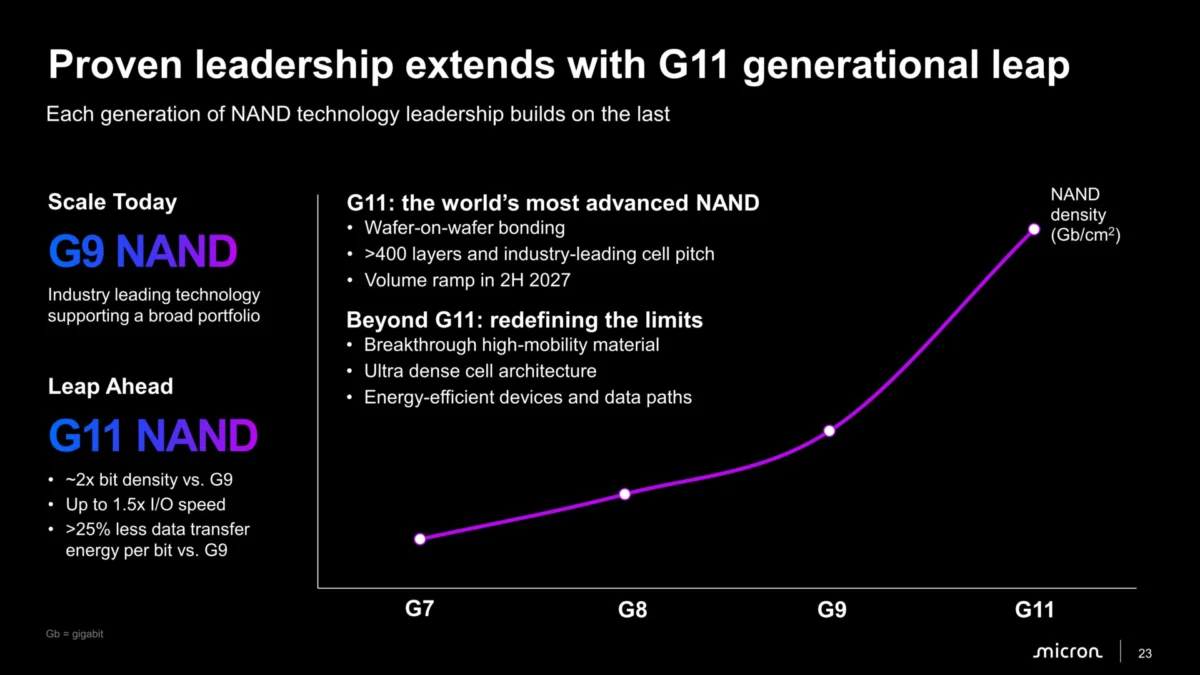
In a surprising move that has sent ripples through the semiconductor industry, Micron Technology has officially bypassed its anticipated "Generation 10" (G10) NAND flash roadmap. During a recent "Technology and Product" webinar, the company confirmed that it is skipping the intermediary step entirely, shifting its focus directly to the development of its G11 NAND architecture. This strategic pivot signals more than just a nomenclature change; it represents a fundamental acceleration in Micron’s efforts to dominate the high-density storage market.
With plans to integrate over 400 layers and deploy a refined manufacturing process, Micron aims to effectively double the bit density compared to its current G9 generation. This bold roadmap suggests that the race for NAND supremacy is entering a new, highly competitive phase.
The Chronology of Innovation: Why Skip G10?
Industry observers are familiar with the practice of "skipping" generations. In the fast-paced world of NAND development, marketing cycles often necessitate a departure from sequential numbering to highlight a "generational leap" rather than an incremental upgrade. For instance, Kioxia and SanDisk famously jumped from BiCS6 to BiCS8, signaling that the technological advancements within the chips were significant enough to warrant a label that suggests a major breakthrough.
Micron’s decision to leapfrog G10 is a calculated response to the rapid maturation of competitor architectures. By moving directly to G11, Micron is signaling that it has achieved a technical threshold that makes the incremental G10 redundant. This shift indicates that the engineering challenges associated with high-layer counts—such as signal integrity, etching precision, and structural stability—have been solved in a way that allows for a larger, more efficient jump in performance and density.
Technical Foundations: The Promises of G11
The transition from G9 to G11 is not merely a numbers game; it is a profound architectural overhaul. Micron has outlined several key pillars that will define this new generation.
Doubling the Bit Density
The most significant metric in the storage industry is, and always has been, bit density. Micron’s current G9 architecture, which powers drives like the Crucial P510, utilizes 276 layers. G11 promises to push this figure to "over 400 layers," a staggering increase of at least 45 percent.
When combined with what Micron describes as the industry’s smallest cell pitch (the physical spacing between memory cells), the company projects a doubling of bit density. While specific metrics can be difficult to verify due to differences in TLC (Triple-Level Cell) versus QLC (Quad-Level Cell) configurations, estimates suggest that if G9 hovered around 21 Gbit/mm², G11 could potentially push that to upwards of 42 Gbit/mm². This level of density would likely outperform current roadmaps for competing architectures, including Kioxia’s BiCS10.
The Adoption of Wafer-on-Wafer (WoW) Bonding
One of the most critical transitions in modern NAND manufacturing is the move toward "Wafer-on-Wafer" bonding. Pioneered by YMTC and subsequently adopted by giants like Kioxia, SanDisk, and Samsung, this technology involves fabricating the memory array and the peripheral CMOS logic circuitry on separate wafers. These wafers are then bonded together to form a single, highly optimized chip.
By adopting this approach for G11, Micron is moving away from monolithic fabrication, which often limits the performance and yield of the logic circuitry. This allows the memory cells to be optimized for density, while the logic (the "brains" of the NAND) can be optimized for speed and power efficiency independently. This process is essential for achieving the layer counts required for a 400+ layer architecture without sacrificing wafer yields.

Interface Speed and Energy Efficiency
Beyond raw capacity, G11 is designed to be faster and more efficient. Micron expects the G11 interface to deliver speeds up to 50 percent faster than its predecessor. With G9 currently operating at 3.6 Gbit/s, G11 is poised to hit the 5.4 Gbit/s mark. While this remains slightly behind Samsung’s projected 5.6 Gbit/s for its upcoming V10 NAND, it represents a substantial leap that will significantly reduce latency in data-intensive applications like AI training and high-performance computing.
Furthermore, Micron is prioritizing sustainability and operational efficiency. The company claims that the energy required to transfer a single bit will drop by more than 25 percent compared to G9. In the context of hyperscale data centers, where power consumption is a multi-million dollar operational expense, such a reduction is a compelling competitive advantage.
Official Responses and Industry Context
Micron’s presentation during its webinar was noticeably confident. Executives emphasized that the G11 roadmap is not a theoretical exercise but a product of years of R&D in materials science and lithography. By explicitly stating that mass production is slated for the second half of 2027, Micron is providing its partners and customers with a clear, albeit ambitious, timeline.
Industry analysts have noted that this move puts significant pressure on the "Big Three" NAND manufacturers—Samsung, SK Hynix, and Micron. Samsung, historically the leader in NAND capacity, is now facing a challenge from both the top (Micron’s density gains) and the bottom (YMTC’s cost-effective production methods). Micron’s G11 strategy appears to be a two-pronged attack: out-innovate the incumbents in density and out-perform them in energy efficiency.
The Future: Beyond G11
While G11 is the immediate focus, Micron has already provided a glimpse into what lies beyond. The roadmap makes explicit mention of an "Ultra Dense cell architecture." While details are scarce, this terminology implies that Micron is working on reducing cell dimensions even further, perhaps approaching the physical limits of current materials.
Perhaps more intriguing is the reference to "Breakthrough high-mobility material." Currently, most NAND flash uses polysilicon channels. These channels are prone to electron scattering, which limits speed and requires higher voltages. A switch to a material with higher electron mobility would represent a fundamental shift in how NAND functions, potentially allowing for even faster switching times and lower power consumption. This hints that after G11, the industry may see a shift away from traditional manufacturing materials toward exotic semiconductors that could redefine storage performance for the next decade.
Implications for the Market
The implications of Micron’s G11 roadmap are profound for several sectors:
- Consumer Storage: Expect to see 8TB and 16TB M.2 SSDs become standard in high-end consumer hardware much sooner than anticipated. The increased bit density will drive down the cost per gigabyte, making large-capacity storage accessible for gaming and creative professional workflows.
- Enterprise and Cloud: The 25 percent reduction in power consumption per bit is a major win for data center operators. As AI models continue to grow, the demand for "hot" storage that can be accessed quickly and efficiently is skyrocketing. G11-based drives will likely become the backbone of next-generation AI server racks.
- Manufacturing Competition: Micron’s aggressive roadmap forces competitors to accelerate their own timelines. We should expect to see announcements from Samsung and SK Hynix regarding their own "next-generation" breakthroughs to prevent Micron from establishing a "first-mover" advantage in the >400-layer category.
Conclusion
Micron’s decision to skip G10 and head straight for G11 is a bold testament to the company’s current engineering trajectory. By focusing on higher layer counts, the adoption of Wafer-on-Wafer bonding, and the promise of future material science breakthroughs, Micron is positioning itself to be the primary engine of innovation in the storage space.
While 2027 may seem like a distant horizon, the preparations for G11 are already underway in fabrication plants across the globe. For the end-user, this translates to faster, more efficient, and incredibly dense storage solutions that will power the next wave of digital transformation. The storage industry is no longer just about keeping data; it is about how fast and how efficiently that data can be accessed, and with G11, Micron is clearly aiming to set the pace for the years to come.