
In the high-stakes arena of semiconductor manufacturing, the landscape has fractured into two distinct realities. On one side stands TSMC, the undisputed titan of the silicon industry, currently enjoying an unprecedented era of profitability and expansion driven by its 3nm process family. On the other side, Samsung Foundry finds itself caught in a cycle of technical skepticism and commercial hurdles, struggling to convince global chip designers to adopt its advanced nodes.
As the industry pushes toward the era of 2nm, the chasm between these two giants has never been more pronounced. While TSMC acts as a financial powerhouse, reinvesting its record-breaking 3nm revenues into a massive expansion of its manufacturing footprint, Samsung is forced to pivot, looking to keep its older 4nm and 5nm lines alive while facing a market that remains wary of its next-generation promises.
The Core Facts: A Market in Disparity
The semiconductor foundry market is currently defined by a "winner-takes-all" dynamic. TSMC holds de facto hegemony in the 3nm class. Its N3 process has become the gold standard for high-performance computing, mobile application processors, and AI accelerators. The revenue generated from this node is not just a success metric; it is the engine for TSMC’s future, funding the R&D and capital expenditure required to bring 2nm and beyond to market.
Conversely, Samsung Foundry’s situation is more nuanced. While the company’s 4nm node is operating at high capacity with satisfactory yields—a rare bright spot in their recent history—the company has struggled to translate this success into momentum for its 3nm and upcoming SF2 (2nm) processes. Many potential clients, deterred by rumors of poor yields and high production costs associated with Samsung’s initial Gate-All-Around (GAA) implementations, are opting to stay with proven, albeit older, nodes or move their business to TSMC.
A Chronological Perspective: From 3nm Hopes to 2nm Hesitation
To understand the current tension, one must look back at the introduction of the 3nm node.
- 2022: Samsung makes a bold move, becoming the first foundry to mass-produce 3nm chips using the GAA transistor architecture. It was intended to be a "leapfrog" moment to overtake TSMC.
- 2023: The "3nm Disaster" narrative begins to take hold. Despite the technological achievement, the yield rates reportedly remain low. The primary consumer of Samsung’s 3nm output is, effectively, Samsung itself.
- Early 2024: TSMC solidifies its dominance. With N3 yields maturing rapidly, the company experiences a "growth explosion," with 3nm products accounting for a massive 33% of its total revenue.
- Late 2024: Samsung pivots its strategy. Recognizing the difficulty in winning over external clients for SF2, the company begins heavily promoting its 5nm and 4nm nodes as cost-effective, reliable alternatives for customers who do not necessarily require the extreme density of 2nm.
This timeline reveals a critical failure of adoption for Samsung. While they have solved the manufacturing challenges of the past, the lack of external "anchor customers"—the big-tech firms that bankroll a foundry’s transition—has created a financial vacuum.
Supporting Data: The Financial Engine of TSMC
The financial gulf between the two manufacturers is best illustrated by their recent quarterly reports. TSMC has reported a staggering 69% increase in profit, largely driven by the premium pricing and high volume of its 3nm output.
The Scale of Expansion
TSMC’s reaction to the demand for N3 has been nothing short of aggressive. Breaking with its traditional philosophy—which usually dictated that new, advanced-process fabs be built only in Taiwan—the company is currently constructing four new "phases" (factory buildings) dedicated specifically to N3 production.
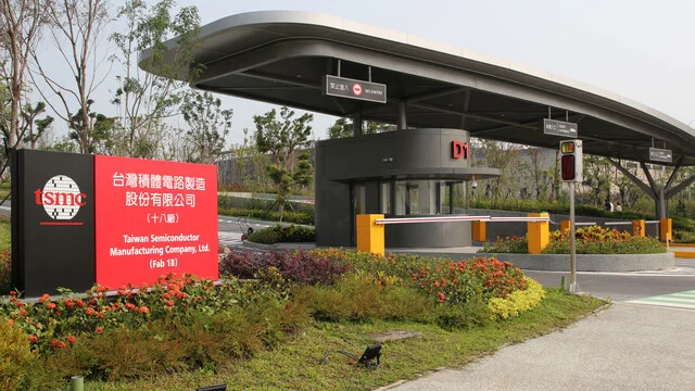
Even more significant is the expansion within Taiwan. Historically, TSMC reserved its domestic facility builds for the next generation of technology (like N2). However, the demand for 3nm has been so overwhelming that TSMC is expanding its Fab 18 facility with two additional phases strictly for N3. This shift indicates that the 3nm node is expected to be a "long-lived" node, serving as the backbone of the industry for years to come.
The Samsung "Foundry Trap"
Samsung’s foundry division, by contrast, continues to struggle with profitability. Because the 3nm process is utilized almost exclusively by Samsung’s own internal product divisions, the foundry lacks the diversified revenue stream that allows TSMC to remain profitable even during cyclical downturns. Intel and Samsung find themselves in a similar boat: the massive capital expenditure required to stay at the cutting edge is not being sufficiently offset by third-party design wins.
Official Responses and Industry Sentiment
While official PR channels often speak of "improving yields" and "strong customer interest," the reality on the ground—as reported by industry analysts and supply chain sources—is more guarded.
Samsung has consistently maintained that its SF2 (2nm) process will be competitive. However, the market’s reaction has been one of skepticism. When a company experiences a "black hole" of investment—where billions are spent on R&D without a corresponding influx of external client orders—it loses the trust of fabless semiconductor companies.
Companies like Apple, NVIDIA, and AMD operate on razor-thin margins and strict launch schedules. They cannot afford the risk of a low-yield process node. For these firms, TSMC is not just a supplier; it is a safe bet. Even if Samsung’s 2nm technology theoretically matches TSMC’s, the risk of supply chain disruption caused by yield volatility is a deterrent that Samsung has yet to fully overcome.
Implications: The Future of the Foundry Industry
The implications of this market structure are profound and will likely shape the electronics industry for the next decade.
1. The Consolidation of Innovation
TSMC’s financial dominance allows it to iterate faster. By the time a competitor solves the issues of one node, TSMC is already two steps ahead in mass production. This creates a "flywheel effect" where the most profitable companies (NVIDIA, Apple) flock to TSMC, providing them with more data, more feedback, and more capital, which in turn leads to a superior next-generation process.
2. The Risk to Samsung’s Foundry Division
Samsung faces a structural crisis. To compete with TSMC, it must either subsidize its foundry costs through its memory and consumer electronics divisions—a move that is increasingly unpopular with shareholders—or it must secure major external clients. If Samsung fails to win a "tier-one" external customer for its SF2 process, the foundry unit may face downsizing or a pivot toward more niche, specialized processes rather than chasing the absolute leading edge.
3. Geopolitical and Strategic Diversification
The reliance on a single entity (TSMC) for the world’s most advanced silicon has become a geopolitical concern. Governments in the US, Europe, and Japan are pouring billions into Intel and local foundry efforts to reduce this dependence. However, the data shows that money alone cannot buy the "yield maturity" that TSMC has cultivated over decades.
4. The Longevity of Older Nodes
One positive implication of this shift is the newfound appreciation for 4nm and 5nm nodes. As the cost of designing for 3nm and 2nm skyrockets, many companies are finding that "mature" nodes offer the best price-to-performance ratio. Samsung’s pivot to these nodes, while a retreat from the absolute leading edge, may actually be a sound business strategy for long-term sustainability.
Conclusion: A Tale of Two Strategies
The current state of the foundry industry is a testament to the fact that, in the world of high-end manufacturing, success is not just about the physics of the transistor; it is about the economics of the ecosystem. TSMC has successfully created an ecosystem that thrives on the 3nm node, turning a singular technical achievement into a global manufacturing juggernaut.
Samsung remains a formidable player, but its struggle to transcend the "3nm disaster" serves as a warning to the entire industry. Innovation without adoption is merely an expense. As we move into the 2nm era, the question for Samsung is no longer just about whether they can manufacture a smaller transistor, but whether they can restore the trust of a global market that is increasingly voting with its capital—and that capital is currently flowing, almost exclusively, toward the halls of TSMC.