
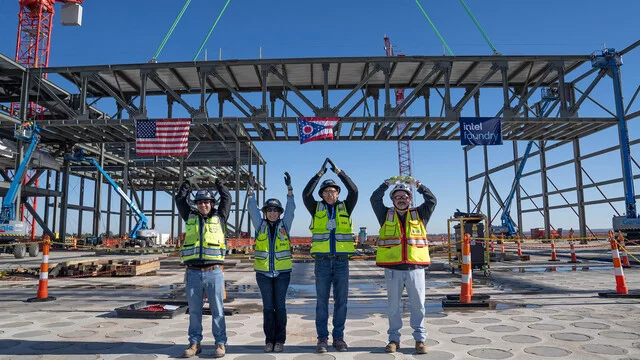
In an industry defined by nanometer-scale precision and billion-dollar gambles, Intel is currently navigating one of the most transformative—and volatile—periods in its history. As the semiconductor giant attempts to pivot its business model toward the "Intel Foundry" strategy, the physical manifestation of this vision is taking shape in Arizona and Ohio. Recent updates from Intel leadership confirm that while construction has faced significant headwinds, the company is finally clearing major milestones at its two most critical manufacturing sites: Fab 62 in Arizona and the massive Ohio One campus.
Despite these advancements, the reality remains that Intel’s manufacturing capacity will not see meaningful relief for several years. For investors, stakeholders, and the broader tech industry, these facilities represent more than just concrete and steel; they are the pillars upon which Intel hopes to reclaim its mantle as the world’s leading chipmaker.
1. Main Facts: The State of the Expansion
Intel’s current infrastructure strategy is split between augmenting existing hubs and building entirely new centers of excellence.
Fab 62 (Arizona): Situated adjacent to the operational Fab 52, Fab 62 is now firmly in the "tool-in" phase. This is a critical transition period in semiconductor manufacturing where the "shell" (the building itself) is handed over to process engineers to begin installing the ultra-precise lithography machines and chemical vapor deposition tools required to etch chips. Intel has confirmed that construction is essentially complete, and the facility is now being prepared for operational ramp-up. The company is currently targeting the end of 2028 for the commencement of high-volume manufacturing.
The Ohio Mega-Site: The project in Licking County, Ohio, represents the largest single investment in the state’s history. After a series of delays caused by shifting market conditions and internal financial restructuring, the project has entered a new, visible phase. The installation of the primary steel girders for the roof structure is underway. While this signals a move toward closing the "shell," the facility remains in the early stages of its lifecycle. Unlike the Arizona project, which is nearing equipment readiness, the Ohio facility is still years away from production, with industry analysts and internal timelines suggesting that a 2029 or 2030 start date is the most realistic scenario.
2. A Chronology of Ambition and Delay
To understand the current state of Intel’s manufacturing, one must look at the timeline of the "IDM 2.0" strategy launched by CEO Pat Gelsinger.
- 2021: The Strategic Pivot. Intel announced a massive capital expenditure program, aiming to revitalize its manufacturing prowess through the launch of Intel Foundry. Plans for the Arizona and Ohio sites were solidified as the bedrock of this expansion.
- 2022–2023: The Financial Chill. As the post-pandemic semiconductor market cooled and Intel’s balance sheet faced pressure, the company was forced to "pause" or "freeze" several expansion projects. Construction at various sites slowed to a crawl as the company sought to conserve cash and re-evaluate its global supply chain needs.
- Late 2024: After several quarters of uncertainty, Intel officially recommitted to its major U.S. construction projects. The resumption of work at Fab 62 and the visible progress on the roof structures in Ohio signal that the "freeze" has officially thawed.
- 2028–2030: The Target Horizon. Intel’s roadmap now points to these dates as the inflection points where the company hopes to reach a new steady state of production capacity, utilizing its most advanced nodes, such as the Intel 14A process.
3. Supporting Data: The Complexity of Semiconductor Scaling
Building a modern "fab" (fabrication plant) is arguably the most complex engineering challenge on Earth. A single facility can cost upwards of $20 billion, with the cost of individual machines—such as ASML’s High-NA EUV scanners—running into hundreds of millions of dollars each.
The Tool-In Process
Once the cleanroom is established—a environment thousands of times cleaner than an operating room—the "tool-in" phase begins. This involves:
- Vibration Isolation: Ensuring the foundation can support tools that detect movement at the atomic level.
- Utility Integration: Routing massive amounts of ultrapure water, specialty gases, and electricity.
- Cleanroom Commissioning: A process that can take months to ensure zero particulate contamination.
The 14A Advantage
Intel has indicated that the Ohio site is being prepared to accommodate the Intel 14A process. This node is expected to be a significant leap forward in power efficiency and transistor density. By the time Ohio comes online, Intel anticipates that the market demand for AI-driven processors will have shifted, requiring the high-density capabilities that only a 14A-class facility can provide.
4. Official Responses and Leadership Vision
The public discourse surrounding these sites has been carefully managed by Intel’s leadership. Naga Chandrasekaran, Executive Vice President of Intel Foundry, recently took to social media and official press releases to reassure the industry.
In his recent update, Chandrasekaran noted: "Building semiconductor leadership requires both innovation and the manufacturing capacity to bring it to scale. We are making steady progress in our U.S. footprint, specifically with the advancements at our Ohio site and the operational preparation of Fab 62."
This sentiment was echoed in a formal statement regarding the Arizona facility: "Today, I am pleased to share that construction and tool installation at Fab 62 are now fully underway, and we expect operations to begin by the end of 2028."
These statements serve a dual purpose: they provide transparency to shareholders worried about the pace of expansion, and they signal to potential foundry customers—who might consider using Intel’s services to manufacture their own chip designs—that the company’s manufacturing roadmap is once again on track.
5. Strategic Implications: Navigating a Tight Market
The urgency behind these builds is not merely academic. Intel has been struggling to keep pace with demand for its processors for several quarters. With internal capacities pushed to the limit, the company has had to adopt a "dual-sourcing" strategy to remain competitive.
The Chiplet Strategy
Intel is increasingly relying on a hybrid approach for its latest consumer lineups. Products such as Intel Panther Lake and the upcoming Intel Nova Lake utilize "chiplets"—modular pieces of silicon that are manufactured by different entities. In many cases, Intel designs the core architecture but offloads the manufacturing of specific components to TSMC, while keeping other critical, proprietary logic production in-house.
The Competitive Landscape
This reliance on external foundries like TSMC highlights the critical importance of getting Fab 62 and the Ohio site online. As long as Intel remains dependent on third-party manufacturers, its margins remain exposed to the capacity constraints and pricing power of those competitors.
Furthermore, the geopolitical climate has made domestic manufacturing a national security priority. By building in Arizona and Ohio, Intel is aligning itself with the U.S. CHIPS and Science Act objectives, positioning itself as a primary beneficiary of federal subsidies intended to decouple the U.S. tech industry from heavy reliance on East Asian supply chains.
Looking Toward 2030
The roadmap is clear, but the path is narrow. Intel’s success depends on three factors:
- Execution: Avoiding further construction or tool-installation delays.
- Yield: Successfully ramping up the 18A and 14A nodes to high-yield volumes.
- Market Adoption: Convincing external clients to utilize Intel Foundry services, ensuring these massive facilities have sufficient order volumes to remain profitable.
In conclusion, the visual progress at Fab 62 and the Ohio site serves as a tangible indicator that Intel is moving out of its defensive "pause" phase and back into an era of expansion. While the fruits of this labor will not be seen on store shelves for several years, the foundation laid today is essential for Intel’s survival in the hyper-competitive landscape of the late 2020s and early 2030s. The industry will be watching closely as the next phase—the high-stakes transition from construction to silicon production—begins to unfold.