
By Editorial Staff
For years, the semiconductor industry has been obsessed with the “TSMC problem”—the reality that the world’s most advanced AI chips are almost exclusively manufactured by a single foundry in Taiwan. However, as the global demand for generative AI and high-performance computing (HPC) continues to skyrocket, Nvidia has realized that the threat to its dominance does not lie solely in the lithography machines of TSMC. The true danger, and the potential failure point for the next decade of computing, lies in the complex, often overlooked ecosystem of substrates, advanced packaging, testing, and optical interconnects.
At the GTC 2026 conference in Berlin, Nvidia unveiled a comprehensive, multi-year strategic roadmap designed to insulate its supply chain from future disruptions. By deploying billions of dollars in capital expenditure, Nvidia is no longer just a chip designer; it is actively architecting the global industrial capacity required to feed its relentless growth.
The Strategic Shift: Beyond the Foundry
Historically, fabless companies focused on the design and left the logistics of the supply chain to their manufacturing partners. That model is now obsolete. Nvidia’s leadership has acknowledged that the "bottleneck" is shifting downstream. As chips become larger and more complex—utilizing heterogeneous integration and chiplet architectures—the demand for high-end substrates and packaging has reached a critical juncture.
Nvidia’s strategy, which was unveiled under strict embargo at the GTC, aims to increase its available substrate capacity by a factor of 2.5x over the next three years. This is not merely a request for more parts; it is a collaborative industrial expansion involving deep financial ties with the world’s most critical material suppliers.
Chronology of Capacity Expansion: 2026–2030
Nvidia’s roadmap is meticulously timed to align with the release cycles of its upcoming GPU architectures, specifically the "Vera Rubin" platform and its successor, "Rosa Feynman."
- 2026 (The Foundation Phase): Immediate capital injection into packaging and testing facilities. Initial expansion of test sites in Taiwan and early-stage infrastructure work in South Korea with Amkor.
- 2027 (The Scaling Phase): Diversification of testing locations to Singapore to reduce geographic concentration risk. Initial output from expanded substrate facilities begins to hit the market.
- 2028 (The Peak Integration Phase): The year of massive scale. Substrate output from Japan (Ibiden) and South Korea (Samsung Electro-Mechanics) hits full stride. Interposer capacity for next-gen chips increases by 300% via Amkor.
- 2029–2030 (The Optical Revolution): Full-scale transition to Co-Packaged Optics (CPO). Capacity for CPO reaches 30x the current baseline, fundamentally altering how data moves within the rack.
Strengthening the Substrate Backbone
Substrates act as the physical foundation for high-performance silicon, providing the electrical connectivity between the chip and the circuit board. With machine lead times currently exceeding 30 months, any shortage in substrate supply is catastrophic.
Nvidia has secured its future through three primary pillars:
1. Unimicron (Taiwan)
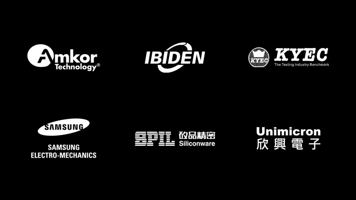
Recognizing the deficit warnings issued by the Taiwanese giant, Nvidia has moved to support Unimicron’s capacity expansion. This partnership is designed to bridge the gap between 2027 and 2028, ensuring that when demand for next-generation platforms peaks, the necessary high-layer-count substrates are available.
2. Ibiden (Japan)
In a move described as a multi-billion dollar capacity reservation, Nvidia is co-financing the expansion of an Ibiden facility in Japan. This project aims to triple the manufacturer’s output, with production slated to come online by 2028. This partnership highlights Nvidia’s strategy of geographic diversification, moving critical infrastructure into stable, high-tech environments.
3. Samsung Electro-Mechanics (South Korea)
Perhaps the most aggressive move involves a long-term supply agreement with Samsung. Nvidia is investing in the expansion of factories in Sejong and Busan. By 2028, Nvidia will consume approximately 25% of Samsung Electro-Mechanics’ entire annual substrate capacity, effectively locking out competitors from a massive portion of the available global supply.
Packaging and Testing: The Hidden Multipliers
If substrates are the foundation, packaging is the structure. As Nvidia’s GPUs grow in size, the need for advanced interposers—the bridge between memory (HBM) and compute dies—has created a shortage in the backend assembly and test (OSAT) sector.
Amkor’s 300% Expansion
The recent news of Amkor’s expansion in South Korea is now revealed to be a joint effort with Nvidia. The company is backing an initiative to increase interposer capacity by over 300% by the end of 2028. This is essential for the "Vera Rubin" and "Rosa Feynman" platforms. By securing this volume, Nvidia ensures that its chips don’t sit idle in a warehouse waiting to be packaged.
The KYEC Investment
Testing is often the "silent" cost of semiconductors. With chips becoming more expensive to manufacture, the cost of a "false negative" or a failure in the field is astronomical. Nvidia has entered into a $1.1 billion agreement with KYEC, a leader in testing equipment. This investment includes a massive capacity reservation in the United States and the utilization of new facilities in Singapore starting in early 2027. By doubling its test capacity by 2027, Nvidia is ensuring that the "quality gate" does not become the bottleneck for shipment volume.
The Next Frontier: Co-Packaged Optics (CPO)
While substrates and packaging are the immediate concerns, CPO represents the future of data center architecture. As the speed of silicon continues to outpace the speed of electrical copper connections, the industry is moving toward light-based communication within the chip package itself.
Nvidia’s partnership with SPIL (a subsidiary of the ASE Group) is perhaps the most forward-looking aspect of the GTC announcements. The agreement focuses on scaling CPO capacity, targeting a 15-fold increase by mid-2027, followed by a staggering 30-fold increase by the end of 2028.
This is not a research project; it is a product-ready mandate. As "Rosa Feynman" moves into mass production toward the end of 2028, these chips will be natively designed for optical interconnects, allowing for massive bandwidth scaling in AI clusters that would be impossible with traditional electrical interfaces.
Implications: The "Nvidia-Centric" Supply Chain
The implications of this massive, multi-year industrial intervention are profound for the semiconductor industry:
- Barrier to Entry: By locking up 25% of major manufacturers’ capacity and co-financing factories, Nvidia has raised the barrier to entry for any competitor. New players will find it nearly impossible to source the substrates and packaging services required to scale a competitive product.
- Geopolitical De-risking: By spreading investments across Taiwan, Japan, South Korea, Singapore, and the USA, Nvidia is insulating itself against regional geopolitical instability.
- Capital Efficiency: While critics might point to the billions in capital expenditure as a risk, Nvidia’s management argues it is the only way to ensure growth. In the world of AI, the cost of being unable to deliver a GPU is far higher than the cost of funding a supplier’s factory.
- The Shift to 2028: The year 2028 emerges as a "super-cycle" in the roadmap. The alignment of expanded substrate capacity, 300% higher packaging output, and 30x CPO capacity suggests that Nvidia is preparing for a step-function increase in AI demand, likely tied to the arrival of systems that require massive optical bandwidth.
Conclusion
At the GTC in Berlin, the message from Nvidia was clear: the era of "just-in-time" supply chains is over. To lead in the age of AI, a company must control the physical industrial process from the substrate level to the final optical connection. Through these multi-billion dollar agreements, Nvidia is not just reacting to the market; it is actively manufacturing the future, ensuring that when the next generation of AI hardware arrives, the infrastructure to build it will be waiting.