
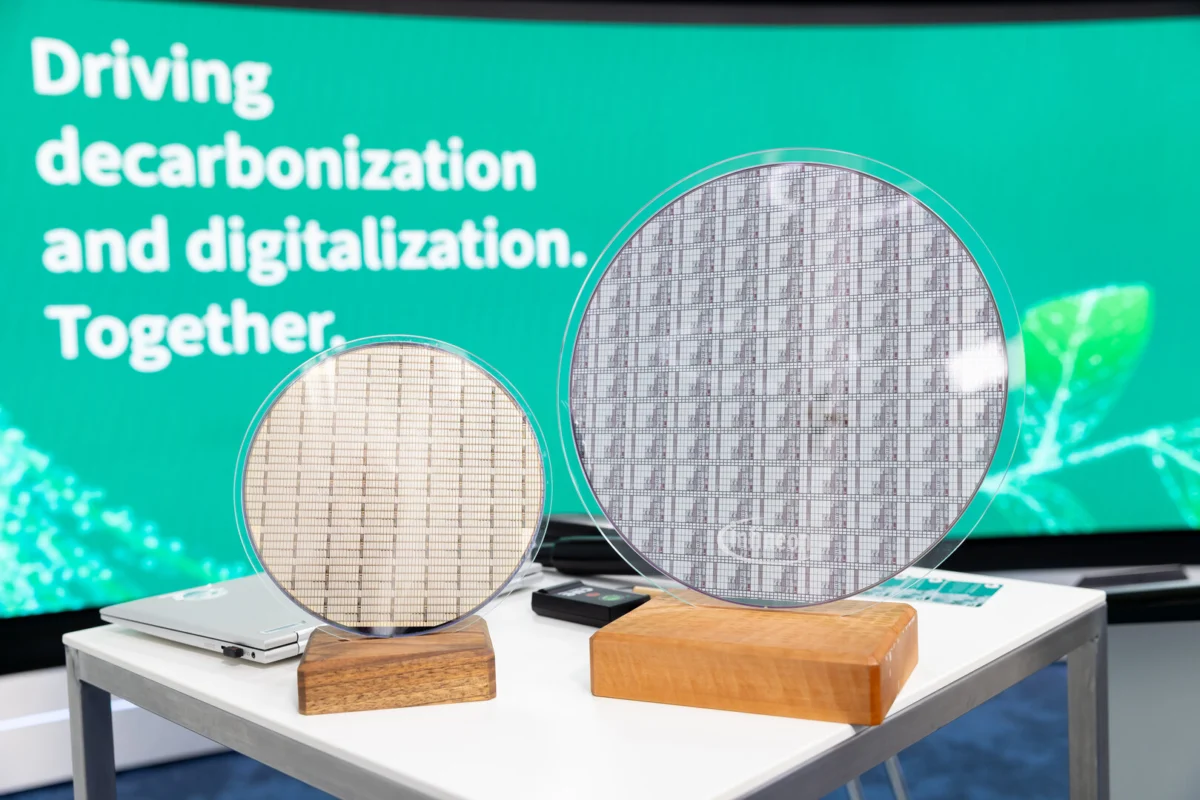
In a landmark move that promises to redefine the landscape of global power electronics, German semiconductor giant Infineon Technologies has announced a massive 1.1-billion-euro investment to establish the world’s first high-volume production facility for Gallium Nitride (GaN) power semiconductors on 300-millimeter wafers. The facility, situated in Villach, Austria, represents a strategic pivot toward next-generation efficiency, positioning Infineon at the vanguard of the global transition toward energy-efficient, high-performance power conversion.
This ambitious project, slated for completion and initial production by the end of 2027, is not merely a manufacturing upgrade; it is a fundamental shift in how the semiconductor industry approaches wide-bandgap (WBG) materials. By scaling up to 300mm wafer sizes, Infineon aims to bridge the long-standing cost gap between traditional silicon and the superior, yet historically more expensive, GaN technology.
The Strategic Core: Scaling to 300mm
The transition from the current standard 200mm (8-inch) wafers to 300mm (12-inch) wafers is the "holy grail" of semiconductor manufacturing efficiency. By increasing the wafer diameter, Infineon can produce 2.3 times more chips per wafer, drastically reducing the cost per unit.
The Villach site is uniquely positioned to handle this transition. Rather than constructing a brand-new facility from the ground up, Infineon plans to integrate this production line into its existing, modernized cleanroom infrastructure. This strategy offers a twofold advantage: it significantly lowers capital expenditure compared to greenfield projects and allows the company to leverage the deep expertise and operational experience of its current workforce in Austria.
A Chronology of Innovation
- October 2023: Infineon accelerates its GaN roadmap by acquiring the Canadian specialist firm GaN Systems for $830 million. This acquisition provided the intellectual property and technical momentum necessary to push GaN toward mass-market feasibility.
- 2024: Following the acquisition, Infineon successfully demonstrates the processing of the world’s first 300mm GaN wafers, proving the technical viability of the scaling process.
- 2025 (Present): Formal announcement of the 1.1-billion-euro investment plan to build the high-volume production line in Villach.
- 2027 (Target): Projected start of full-scale production, bringing 300mm GaN devices to the global market.
- 2034 (Target): Completion of the multi-phase investment horizon, cementing the facility’s role as the central hub for global GaN supply.
Supporting Data: The Rise of Gallium Nitride
The investment is underpinned by robust market projections. According to industry analysis from the Yole Group, the market for GaN power semiconductors is poised for exponential growth. With a projected annual growth rate of approximately 35% between 2025 and 2031, the market is expected to reach a valuation of $3.5 billion by 2031.
Why GaN Matters
Gallium Nitride is a compound semiconductor consisting of gallium and nitrogen. Its physical properties make it vastly superior to silicon for power applications:
- Efficiency: GaN devices operate with significantly lower conduction and switching losses, leading to less heat generation and higher energy efficiency.
- Speed: Higher electron mobility allows for significantly faster switching frequencies, which in turn permits the use of smaller passive components (like inductors and capacitors), enabling smaller and lighter electronic systems.
- Power Density: The material can withstand higher voltage levels and temperatures, making it ideal for the extreme demands of modern AI data centers, electric vehicles (EVs), and renewable energy infrastructure.
The ability to manufacture these components on 300mm lines effectively democratizes the technology. Because the production processes for 300mm GaN share significant commonalities with existing silicon CMOS manufacturing, Infineon can repurpose existing equipment, creating a cost-competitive edge that was previously unattainable for wide-bandgap materials.
Official Perspectives: Sovereignty and Strategy
The investment has received significant support from the Austrian government and aligns with the broader European Chips Act. The European initiative, designed to bolster the continent’s technological sovereignty and reduce reliance on imported components, will contribute approximately 319 million euros in subsidies toward the project.
Jochen Hanebeck, CEO of Infineon Technologies AG, emphasized that this move is central to the company’s vision of the future:
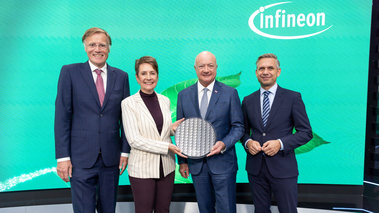
"This substantial investment is our clear commitment to strengthening the European semiconductor ecosystem and Europe’s technological sovereignty. With the establishment of the 300-millimeter high-volume production, we are the first company worldwide to bring Gallium Nitride power electronics into mass production. We are paving the way for the widespread use of GaN in a multitude of key applications, including artificial intelligence, energy infrastructure, electromobility, and robotics. This state-of-the-art facility translates our innovation leadership into immediate customer value."
Hanebeck’s remarks underscore a key industry trend: the shift from "innovation as a novelty" to "innovation as an infrastructure requirement." As AI servers demand more power, and as the global grid transitions toward decentralized renewable sources, the necessity for high-efficiency power management is no longer a luxury—it is a critical bottleneck that Infineon intends to resolve.
Implications: A New Era for Electronics
The implications of this investment extend far beyond the borders of Austria.
1. The AI Power Revolution
Artificial Intelligence models require immense computing power, which in turn places an unprecedented load on data centers. Traditional silicon power supplies are reaching their limits in terms of heat dissipation and power conversion efficiency. By moving to GaN-based power supplies, data center operators can achieve significantly higher power density, reducing energy consumption and, crucially, cooling costs.
2. Electromobility and Robotics
In the automotive sector, GaN is a key enabler for faster, more efficient EV chargers and more compact motor controllers. For robotics, where weight and battery life are critical, the increased power density of GaN components allows for more agile and long-lasting machines.
3. Energy Infrastructure
Solar inverters and grid-scale storage systems are seeing a rapid shift toward wide-bandgap materials. The 300mm production capacity will allow for the mass deployment of solar energy solutions, helping to accelerate the transition to a carbon-neutral energy sector.
4. Competitive Landscape
Infineon’s move sets a high bar for competitors. By locking in the 300mm manufacturing process, they are effectively establishing an economy of scale that will be difficult to challenge in the short term. While other players in the semiconductor industry are exploring GaN, Infineon’s combination of existing silicon manufacturing expertise, the strategic acquisition of GaN Systems, and massive government-backed funding creates a formidable barrier to entry.
Conclusion
The decision to invest 1.1 billion euros into the Villach facility is a definitive statement that Gallium Nitride has "arrived." By moving the technology into the realm of 300mm wafer mass production, Infineon is doing more than just expanding its portfolio; it is rewriting the rules of power electronics. As we look toward the 2030s, the efficiency gains enabled by this technology will be woven into the fabric of the digital economy, from the servers powering our AI to the infrastructure charging our vehicles. With the support of the European Chips Act and a clear technical roadmap, Infineon is well-positioned to dominate this next generation of power semiconductor manufacturing.