
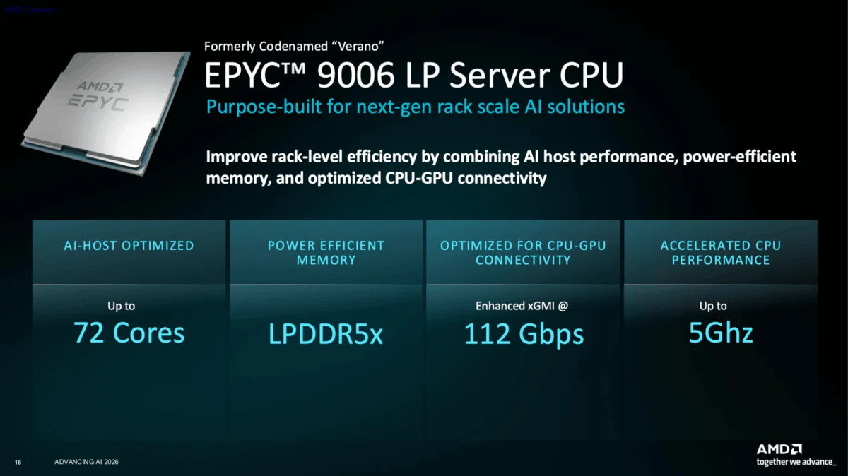
The landscape of high-performance computing (HPC) is undergoing a radical shift as power efficiency becomes as critical as raw processing throughput. AMD, continuing its aggressive expansion within the data center market, has recently provided a glimpse into its upcoming strategy for low-power server architectures. While the industry has been focused on the flagship "Venice" EPYC 9006 processors, a secondary, highly specialized branch—the "Verano" family, marketed as EPYC 9006 LP—is now coming into sharper focus.
Recent disclosures from industry partner Dynatron have effectively confirmed that these specialized chips will utilize a distinct interface known as the SB1 socket. This revelation marks a significant milestone in AMD’s roadmap for 2027, signaling a move toward specialized, BGA-based (Ball Grid Array) architectures designed specifically for the rapidly evolving "rack-scale" AI and cloud infrastructure markets.
Main Facts: The Emergence of the SB1 Socket
The primary development is the identification of the SB1 socket, which differentiates the "Verano" EPYC 9006 LP series from the standard SP7 and SP8 sockets used by the high-performance Venice line.
According to product documentation inadvertently surfaced by cooling solution manufacturer Dynatron, the SB1 interface is being prepared for upcoming thermal management hardware, specifically the "SB1-4U-ACTIVE" cooler. The nomenclature "SB1" is particularly telling; in the context of processor sockets, the "B" likely denotes a BGA package. Unlike traditional land-grid array (LGA) sockets that allow for CPU upgrades and replacements, BGA processors are typically soldered directly onto the motherboard.
This shift toward a soldered, low-power architecture reflects a broader trend in server design where space, thermal footprint, and power delivery efficiency are prioritized over the modularity of standard server CPUs. With a target of up to 72 cores and clock speeds reaching 5 GHz, the Verano series is engineered to deliver high performance-per-watt ratios, likely catering to hyperscale data centers that require high-density, low-power compute clusters.
Chronology of the EPYC 9006 Roadmap
To understand the significance of the Verano/SB1 development, one must look at the timeline AMD has established for its Zen 6 architecture.

- July 2024: AMD officially announces the EPYC 9006 "Venice" series. These processors, featuring up to 256 cores, were the primary focus of the announcement, establishing a new high-water mark for multi-core performance in the x86 ecosystem.
- Late 2024/Early 2025: Technical details regarding the "LP" (Low Power) variants begin to leak. It is clarified that these chips will be a distinct sub-family, aimed at specialized environments rather than general-purpose server workloads.
- Mid-2025: Industry partners, including cooling manufacturers, begin preparing the infrastructure for the next generation. The appearance of the "SB1" socket designation in Dynatron’s database confirms that the hardware foundation for these chips is moving into the validation phase.
- 2027 (Projected): Official launch of the Verano series. This aligns with the integration of SOCAMM2 support, which allows for the use of interchangeable LPDDR5X memory modules, balancing the fixed nature of the processor with the need for flexible memory configurations.
Supporting Data and Technical Architecture
The Verano architecture represents a departure from the "one-size-fits-all" server approach. By leveraging the SOCAMM2 (System on Chip Architecture for Memory Modules) standard, AMD is acknowledging that memory bandwidth is often the bottleneck in modern AI-driven server racks.
Core Specifications
- Processor Family: EPYC 9006 LP (Verano)
- Socket: SB1 (BGA-based)
- Core Count: Up to 72 cores
- Turbo Clock: Up to 5.0 GHz
- Memory Support: LPDDR5X via SOCAMM2 modules
- Target Market: Rack-scale AI solutions and high-density cloud compute
The use of LPDDR5X is a strategic choice. While standard DDR5 offers higher capacity and speed, LPDDR5X significantly reduces power consumption, which is critical when thousands of these chips are packed into a single data center rack. By separating the memory into modules while soldering the processor, AMD is providing a middle-ground solution: the permanence of a soldered CPU for stability and thermal efficiency, with the agility to upgrade memory as AI model requirements grow.
Official Responses and Industry Silos
AMD has been measured in its public disclosures, focusing on the high-level goals of the EPYC 9006 series while leaving the granular details of the LP variants to the ecosystem partners. Dynatron, in particular, has inadvertently provided the most concrete evidence of the SB1 socket’s existence.
While Dynatron’s product pages currently reuse imagery from the J26 (SP7) cooler, the distinct naming of the "SB1-4U-ACTIVE" indicates that internal testing for the new platform is well underway. This is standard operating procedure in the server supply chain; cooling manufacturers receive early access to socket dimensions and thermal specifications to ensure that when the chips launch in 2027, the infrastructure to support them is already available.
Observers have noted that this "leak" is a common occurrence in the enterprise hardware cycle. Manufacturers like Dynatron must list compatible parts well in advance to allow server OEMs (like Dell, HPE, and Supermicro) to integrate them into their chassis designs long before the processors hit the market.
Implications for the Future of Data Centers
The move toward the SB1 socket and the Verano architecture carries profound implications for the industry.

1. The Rise of "Rack-Scale" Computing
AMD has explicitly stated that the Verano series is intended for "rack-scale AI solutions." This suggests that AMD is moving away from the paradigm where a server is an isolated unit. Instead, the rack becomes the computer. By optimizing for lower power, AMD can increase the density of processors per rack, thereby increasing the total FLOPS (floating-point operations per second) available for large-scale AI training and inference.
2. The BGA vs. LGA Debate
The choice of a BGA (soldered) socket for the SB1 platform might initially seem like a setback for users who value upgradability. However, in the realm of hyperscale data centers, CPU replacement is rarely performed on a per-socket basis. Servers are typically retired and replaced in their entirety every 3 to 5 years. By utilizing BGA, AMD can achieve superior signal integrity between the processor and the motherboard, as well as a more compact board design, which is essential for the high-density requirements of modern AI clusters.
3. Competition with NVIDIA
The "Verano" chips are positioned as a direct answer to competing architectures, such as NVIDIA’s "Vera" project. NVIDIA has similarly leaned into BGA-based designs for its specialized compute modules. By adopting the SOCAMM2 standard, AMD is ensuring that it can match the flexibility of these competing systems while maintaining the compatibility and ecosystem advantages of the x86 instruction set.
4. The 2027 Pivot
The 2027 release date is not coincidental. It aligns with the anticipated maturation of LPDDR5X technology and the expected surge in demand for power-efficient AI inference at the edge and in cloud-native environments. AMD is clearly betting that by 2027, the "Venice" chips will continue to dominate the traditional high-performance enterprise space, while "Verano" will carve out a new niche in the high-density, energy-sensitive AI market.
Conclusion
The identification of the SB1 socket serves as a roadmap for where AMD intends to take its EPYC platform. By segmenting the Zen 6 generation into standard "Venice" CPUs and the specialized "Verano" LP line, AMD is demonstrating a sophisticated understanding of the diverse needs of modern data centers.
While the general-purpose market continues to demand more cores and higher clock speeds, the AI and cloud infrastructure sector is demanding efficiency and density above all else. With the SB1 socket and the integration of SOCAMM2, AMD is positioning itself to lead both fronts. As we approach 2027, the industry will be watching closely to see if this bet on BGA-based, low-power architecture pays off in the competitive landscape of rack-scale AI. For now, the "SB1" designation serves as the first tangible piece of a much larger, more efficient puzzle that AMD is currently assembling.