
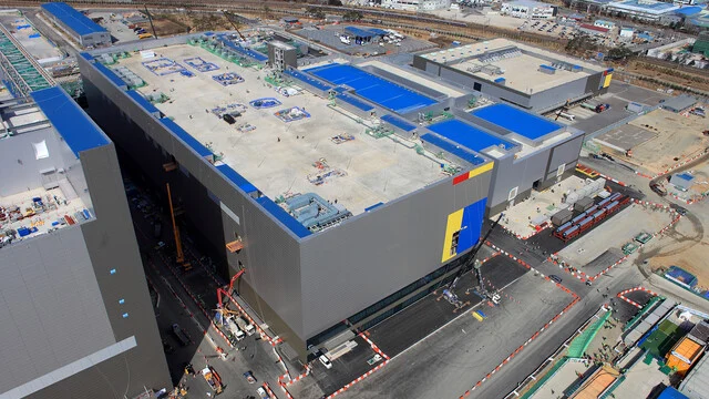
In a move that signals renewed confidence in the global semiconductor market, Samsung Electronics is aggressively accelerating the expansion of its manufacturing footprint at the Pyeongtaek mega-campus in South Korea. Following a period of strategic hesitation caused by global supply chain volatility and fluctuating demand, the tech giant is moving forward with the construction of the "P5" complex, which will consist of two massive, high-capacity fabrication plants (fabs).
This expansion is not merely an increase in physical space; it represents a fundamental shift in Samsung’s manufacturing philosophy, utilizing a new "multi-cleanroom" design that promises to redefine output capacity for DRAM and other memory technologies.
The Core Expansion: P5 Fab 1 and P5 Fab 2
The Pyeongtaek site, already a crown jewel in Samsung’s global semiconductor infrastructure, is currently undergoing a massive transformation. While the "P4" facility continues to be optimized for the latest generation of wafer processing, the spotlight has shifted to the upcoming P5 project.
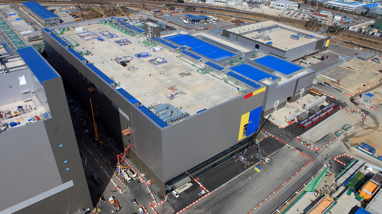
Samsung is preparing to break ground on what is being referred to as "P5 Fab 2," a sister facility to the primary "P5 Fab 1." Both structures are gargantuan in scale, designed to span 661 meters in length and 194 meters in width. The scale of the construction is visible from space, with heavy machinery and a forest of cranes marking the site as one of the most active industrial development projects on the planet.
The New Architectural Paradigm: The 3×3 Cleanroom Design
One of the most critical aspects of this expansion is the adoption of a cutting-edge cleanroom layout. Samsung is moving away from traditional, smaller-scale layouts toward a 3×3 configuration. By stacking or partitioning internal cleanrooms in a 3×3 grid, Samsung expects to boost output capacity by at least 50% compared to previous designs. This design, currently being trialed in the P4 facility, is intended to maximize the utility of every square meter of the massive building footprint.
Chronology of a Strategic Pivot
The path to the P5 project has been anything but linear. Understanding the current acceleration requires a look back at the hurdles Samsung has faced over the past three years.
2021–2022: The Initial Delay
The P5 facility was originally slated for construction over three years ago. However, the semiconductor industry faced a "perfect storm" during this period:
- Foundry Weakness: Samsung struggled to compete with TSMC in the high-end logic chip market, leading to a reallocation of resources.
- Market Slump: A sharp downturn in the memory chip market—driven by an oversupply of consumer electronics and a cooling of the post-pandemic IT boom—forced Samsung to hit the brakes.
- Strategic Stagnation: Major investments in both South Korea and the United States were paused or significantly slowed to protect the company’s balance sheet.
2023–2024: Preparation and Foundation
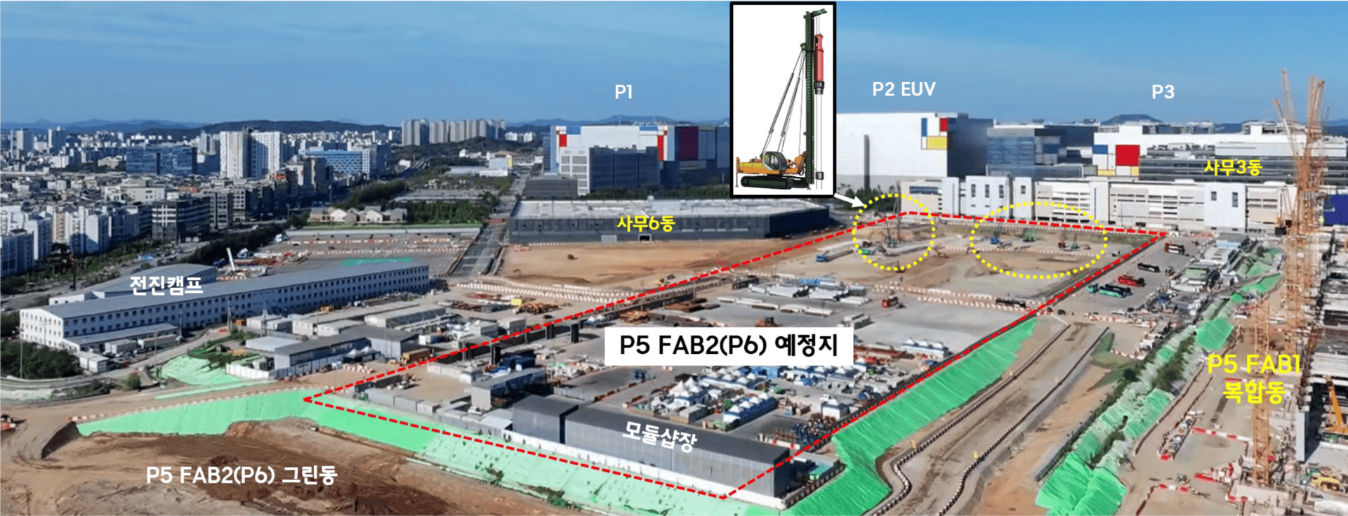
While construction was stalled, Samsung did not abandon the site. Instead, it focused on site preparation and infrastructure groundwork. During this time, South Korean analysts and industry observers, closely monitoring the site through local satellite and aerial imagery, identified that the master plan for the campus always included space for a sixth facility.

2025 and Beyond: The Construction Push
With the global demand for AI-driven high-bandwidth memory (HBM) and next-generation DRAM surging, the market outlook has fundamentally changed. Samsung has brought in the heavy equipment necessary for deep-pile driving, signaling that the "Dornröschenschlaf" (sleeping beauty phase) is firmly over.
Supporting Data: The Scale of Ambition
The sheer volume of wafers that Samsung intends to produce by the mid-2030s is staggering. To understand the significance of the P5 project, one must look at the current production numbers.
- Current Capacity: Samsung’s existing DRAM production capacity is estimated at approximately 650,000 wafers per month.
- The P5 Impact: Upon reaching full operational status, P5 Fab 1 and Fab 2 are projected to each contribute up to 300,000 wafers per month.
- Effective Doubling: Once the P5 complex is fully functional, Samsung will effectively double its current DRAM manufacturing capacity.
Projected Timeline:
- 2028: Initial production lines expected to come online in Fab 1.
- 2029: Initial production lines expected to come online in Fab 2.
- Mid-2030s: Final completion and full-scale capacity realization.
This aggressive timeline mirrors the broader industry trend. Competitors like SK Hynix have also announced plans to triple their production capacity by 2034, leading to a "race to the top" in manufacturing capability that will likely shape the global memory market for the next two decades.
Official Stance and Market Implications
Samsung has maintained a professional, forward-looking stance regarding these expansions. Through recent corporate communications and a detailed promotional video released to stakeholders, the company has highlighted the Pyeongtaek campus as the backbone of its "Future-Proofing" strategy.
The video underscores the logistical complexity of the site, showcasing the four existing, fully operational factories and the active construction zones. By emphasizing the integration of the P4 and P5 projects, Samsung is signaling to investors that it is not just adding capacity, but upgrading its technological efficiency.
Economic and Strategic Implications
- Supply Chain Dominance: By doubling its capacity, Samsung aims to maintain its status as the world’s leading memory manufacturer, ensuring it can meet the insatiable appetite for memory in AI data centers, autonomous vehicles, and high-performance computing (HPC).
- Technological Superiority: The 3×3 cleanroom design is not just about quantity; it is about efficiency. By integrating more advanced photolithography tools into larger, more modular cleanrooms, Samsung reduces the cost-per-wafer and increases yield rates for complex, multi-layered NAND and DRAM products.
- Regional Economic Impact: The expansion solidifies Pyeongtaek as the global epicenter of semiconductor manufacturing. The project supports thousands of high-tech jobs and forces a massive upgrade in the surrounding infrastructure, from power grid requirements to chemical supply chain logistics.
Challenges Ahead
Despite the optimism, the road to the mid-2030s is not without risks.
- Geopolitical Volatility: As trade tensions between the US, China, and South Korea continue to simmer, Samsung must navigate a complex web of export controls and regional restrictions.
- Capital Expenditure (CapEx) Risks: Constructing and equipping these massive fabs requires hundreds of billions of dollars. If the memory market experiences another cycle of extreme volatility, the pressure on Samsung’s profit margins will be significant.
- Talent Acquisition: Building the physical shell is only half the battle. Operating these facilities requires a constant pipeline of highly skilled engineers and technicians, a resource that is currently in short supply globally.
Conclusion
The expansion at the Pyeongtaek campus represents a massive, calculated bet on the future of technology. By transitioning from a "growth-through-iteration" model to a "growth-through-scale" model with its new P5 facility design, Samsung is positioning itself to be the primary supplier for the AI era.
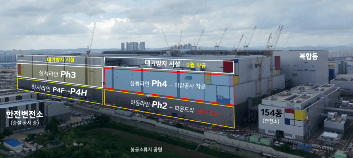
While the road to completion is long, the transition from empty lots to the current state of heavy construction proves that Samsung has returned to its roots of aggressive, large-scale investment. For the semiconductor industry, the message is clear: the P5 complex is not just another factory—it is the cornerstone of the next decade of digital infrastructure.